I’ve been working on a new project using the Intel Atom processor and 945GSE chipset. In the platform design guide that Intel published they have various recommendations for routing traces to the corners of BGA PCB footprints for the parts and I was curious as to why these were being recommended. It turns out I’ve been fortunate in my past experience with RoHS-based designs since most of the boards I work on are small, fairly rigid (most are 1.6mm thick) and the BGA components were few and of fine pitch. However, there is an ugly failure mode with RoHS process boards and BGA’s which has come to be known as “pad cratering”. This is a bit of a misnomer, since the “crater” is the space left vacant when a BGA ball pad lifts off the board.
Causes of pad cratering
Simply put, pad cratering is merely the failure of the resin bond between the board and the surface ball pads of a BGA footprint. This has been exacerbated by RoHS because of the higher reflow temperatures needed (embrittles the resin) and the greater hardness of RoHS compliant solders. There are at least two main causes: mechanical stress due to thermal cycling of the board during reflow, and stress on the joints caused by board flexing during handling and other mechanical shocks. The failures normally begin at the outside corners of the BGA package and may not be apparent at first if the connecting traces to the pads don’t immediately fracture. The most common electrical failure point is at the perimeter of the ball pad where a routing trace connects to the pad.
Dealing with pad cratering
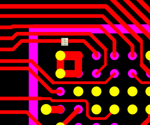
Note that this heading does not say “preventing pad cratering” as it appears that simply attempting to prevent pad cratering will not yield significant increases in board reliability. The most extreme example I’ve seen in the attempt to prevent pad cratering is to apply epoxy to the 4 corners of each BGA package to provide mechanical stress relief for the corner pads. For most of us however that’s simply not practical. What has apparently been working for me is to break out the corner BGA pads and those of the next row back on the diagonal with trace widths equal to the diameter of the ball pads.
In this view the yellow shapes represent pads with a 4mil via-in-pad blind via connecting to the second layer, purple pads do not have vias. Via-in-pad was mentioned in one study I read as another possible way to mitigate pad cratering but that not enough research had been done to determine its effectiveness. The idea behind the wide traces at the pad is to eliminate copper trace fracturing at the pad perimeter. Evidently the dual approach of using fat traces plus via-in-pad has worked for me as none of the boards on which I’ve used this approach have yet to experience a failure due to pad cratering. These boards are only 0.8mm thick and are used in a hand-held product, unfortunately a prime candidate for pad cratering failure. But so far so good…
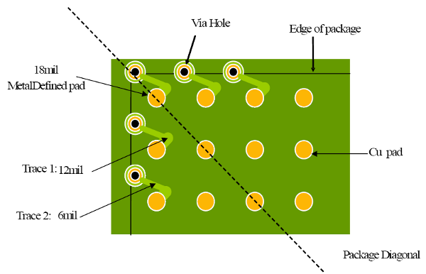
It’s been suggested that for attaching traces to the corner ball pads one should route away from the pad at a 45 degree angle relative to the pad with a wide trace for about 1.2mm, then neck down to normal routing width and go off in the direction of the route. The image below illustrates this:

Using short fat trace stub to mitigate pad cratering
Another approach to reducing the stress at the pad to trace boundary is to use solder mask defined pads rather than metal defined pads for the entire array. Jon Manning (you can find him on Linkedin) suggested using solder mask defined pads for the first 3 rows in on the diagonal, using the same solder mask size as pad metal size for the balance of the array, and increasing the pad metal size in the corners appropriately. Depending on the ball pitch of your parts and your board layer structure it seems that some combination of these approaches should work for you to sufficiently mitigate the effects of pad cratering. Since shock and flexing are a significant contributor to pad cratering that’s one place the mechanical design group can make contributions. We don’t use solder mask defined pads on all ball pads as a rule since metal defined pads appear to have somewhat highter soldering reliability and less problems with joint cracking.
Nicholas Vickers, Kyle Rauen, Andrew Ferris and Jianbiao Pan of Cal Poly State University published a study of BGA soldering reliability. Their research conclusions can be found here. Also, thanks to Jon Manning for sharing his considerable pcb design experience.
-Jeff

comment_form