These are just some of my personal takeaways from Computex 2025 here in Taipei, Taiwan. This is not a comprehensive review of the mother of all Asian trade shows, just some notes about things I’m interested in. I got to attend Jensen Huang’s keynote speech this year. Wow, what a difference a year makes! Last year the hype was on full bore, announcement of the Blackwell GPU’s and all kinds of possible applications for AI, a few were pretty creepy to some folks, but mostly all just smoke and mirrors.
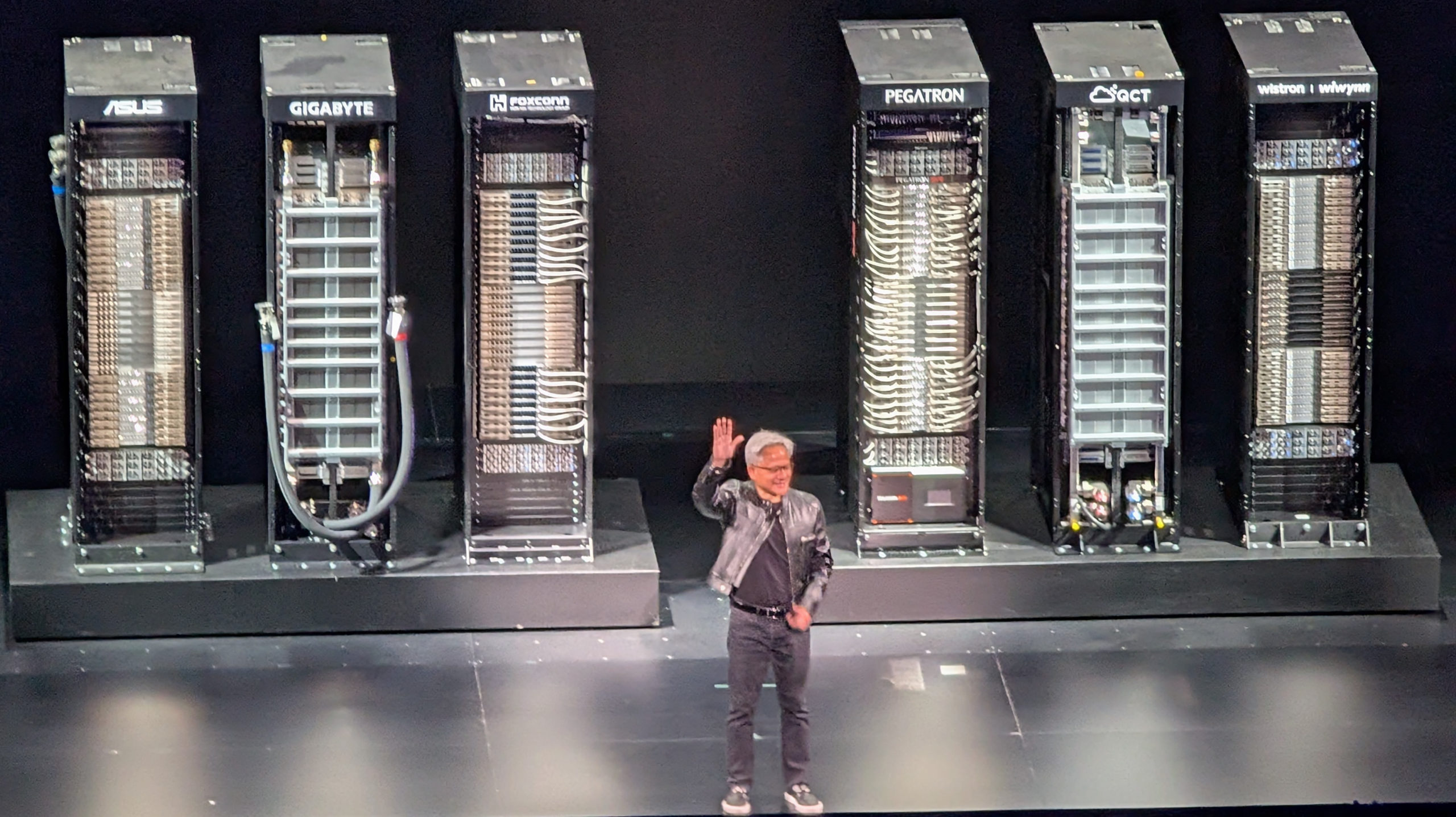
This year there was none of that. The presentations (and Huang himself) were considerably more subdued, but instead of hype we actually saw real hardware, real applications and real results from applied AI, particularly Nvidia’s Omniverse, their operating system for 3D simulation.
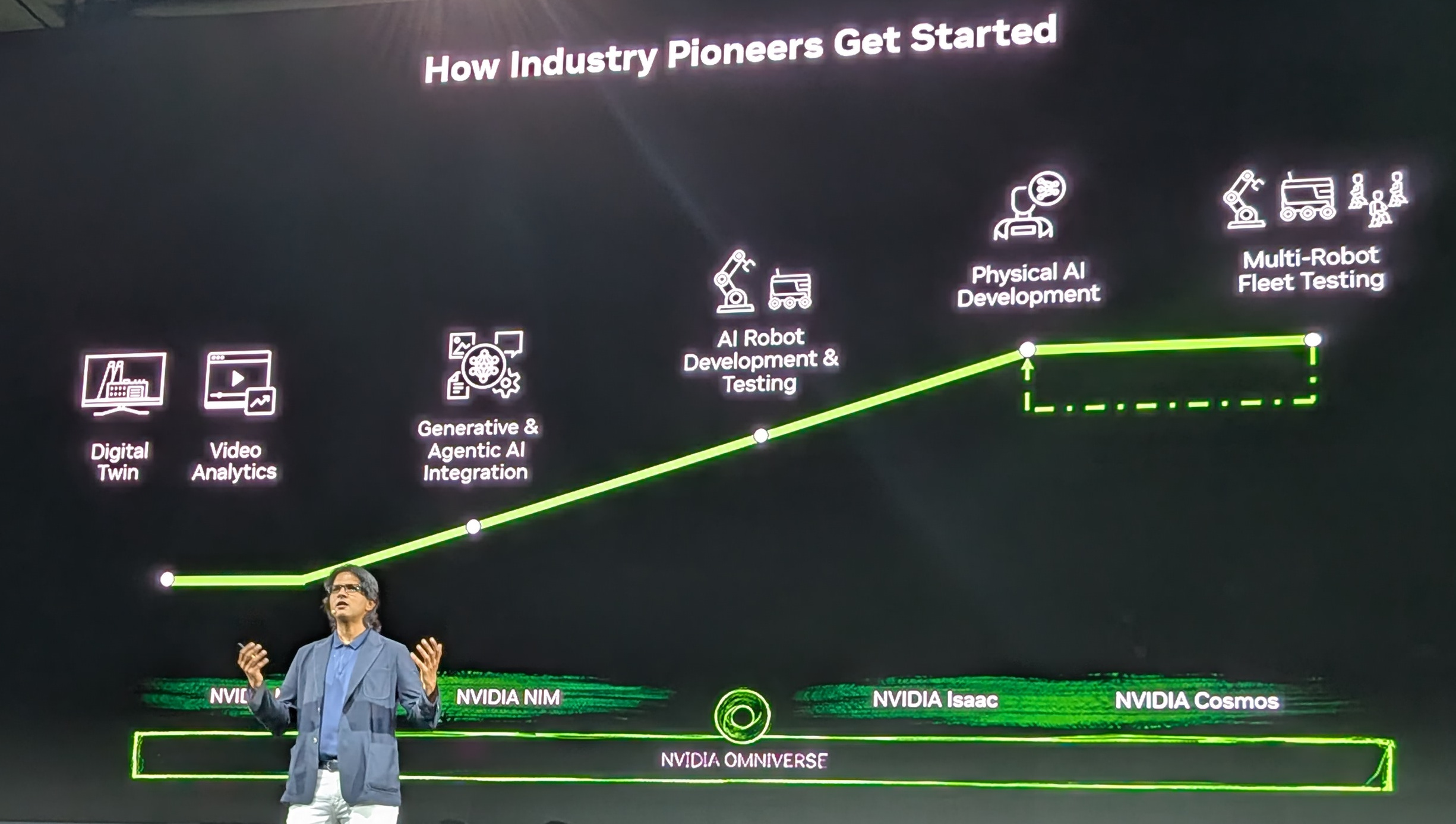
Deepu Talla from Nvidia said that physical AI and 3D simulation have reached a tipping point. Nvidia Omniverse is the operating system for simulation of physical problems. This combination of physical AI and simulation has come about within the last 12 months. Foundation models for robotics physics are very limited currently. Synthetic data generation is needed to aid simulation. Robotics needs extremely accurate data. Using generative AI can generate the data, while Omniverse combines synthetic data with real world data in order to drive robots. Robots gather real world data with sensors in order to improve their performance. He noted Foxconn’s use of Omniverse to simulate the design of new factories was probably the largest deployment of Omniverse to date.
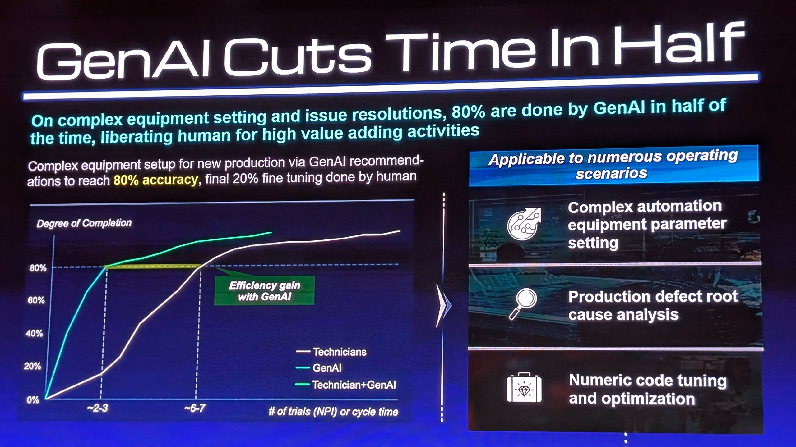
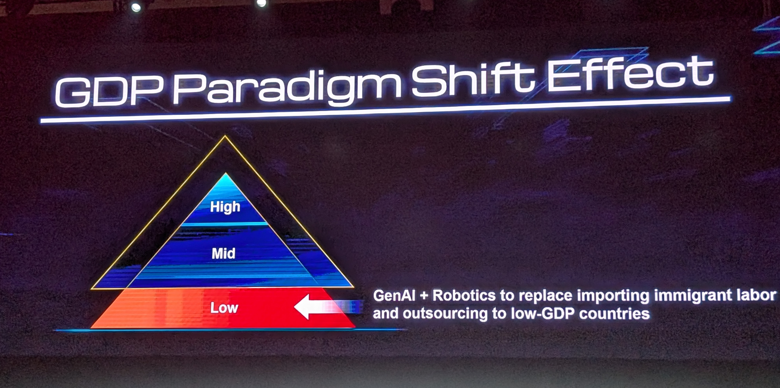
Foxconn’s chairman, Young Liu, described in detail in a forum after Huang’s keynote how Foxconn has used Omniverse to simulate designs of their factories. The creation of a fully synthetic simulation “digital twin” of a factory helps implement not only the building and equipment layout but also simulation of how the robots that are needed will work and then using the results of simulations to actually program those robots. This saves months of planning and construction time. Foxconn’s goal is to have robots do 80% of tasks while 20% of remaining tasks beyond robotic capabilities are done by humans. Labor shortages are driving Foxconn’s deployment of robots. All this has taken place within the last year and a half. Young says the great challenge for countries is the replacement of low GDP work with generative AI as the world is running out of low GDP countries.
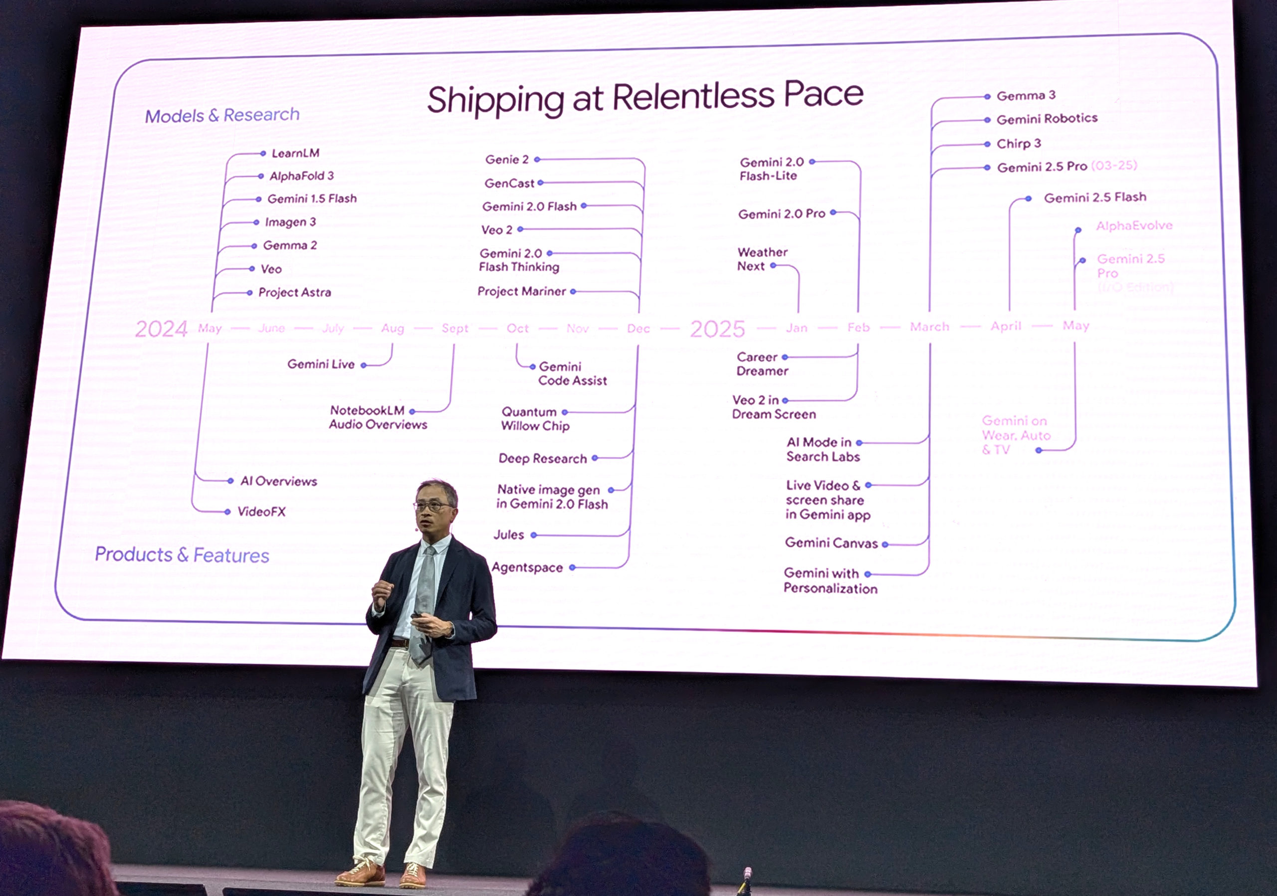
Ed H. Chi from Google noted that Google Gemini has gone from processing 9.7T (terra-tokens) per month to 480T tokens per month in just one year. Referring to the Google Deepmind project, in the past separate models were required depending on each task at hand. But now all of these models have been compressed into a single large model. Maybe this is just marketing hype, but Chi claims this is the biggest advance in computer science in the last 10 years.
Jens Hinrichsen from NXP said that physical AI has to move to the “edge” because of all the data being generated. AI plus IOT is the way forward. Context processing at the edge is needed to extract the true value from data and discard that which is of no value, much like the way our brains work. There’s simply not enough internet bandwidth to send everything from the edge to the cloud for processing there.
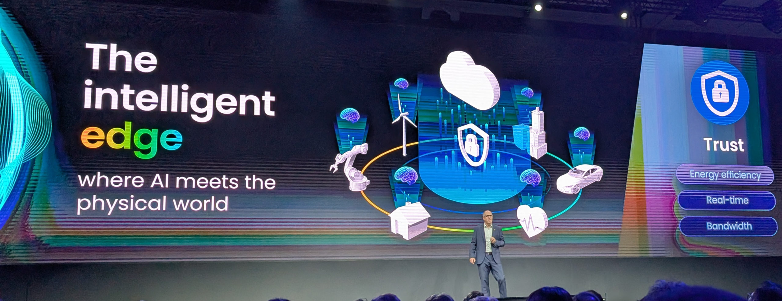
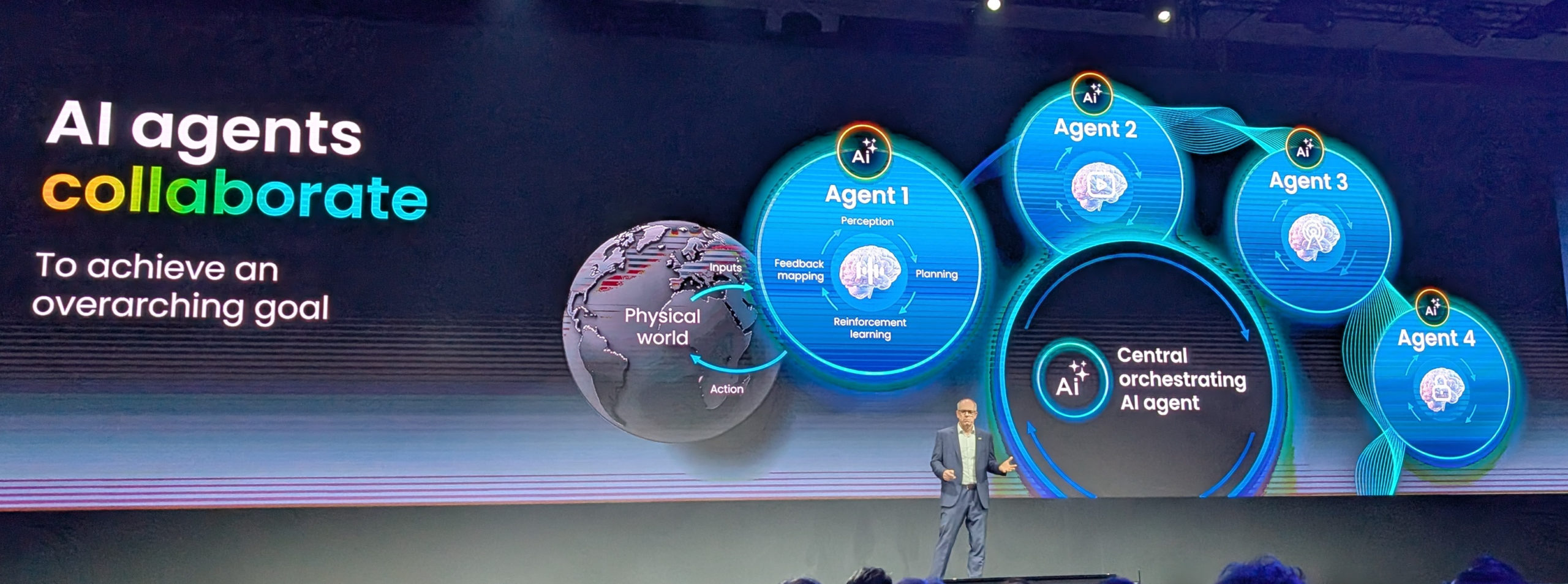
Within the last year Agenic AI has become a reality- edge devices have become autonomous, there’s no need for the cloud in order to allow edge devices to sense, think and act on their own. But the edge and the cloud will always coexist. AI agents can learn and adapt to situations. But a very large challenge is providing a high level of control reliability, safety and cyber security.
I think the real “killer app” for AI has finally become obvious: management of vast amounts of data in order to extract value. “Digital Twin” is not exactly a new concept, we’ve been doing that for many years in product development, creating a fully synthetic 3D functioning model of a product before cutting any tooling. But doing it on this kind of scale and enabled with AI plus physical data is new. It’s nice to see genuine high value applications finally emerging at last from all the past hype around AI. However, the 800 pound elephant in the room is still with us. Power requirements to run AI “factories” are outpacing the planet’s ability to generate electricity. Last year’s Nvidia Grace Blackwell 100KW rack has morphed into this year’s Blackwell 160KW rack. Even edge devices are becoming more power hungry as their processing power increases. Those of us in Taiwan, where they’ve just shut down the nation’s last nuclear reactor, may soon have to make hard choices between AI and AC.