OMAP Noisy NTSC/PAL Video Issues.

The Orion project, mentioned in another post here, has video output capabilities like the Nokia N900 and other smart phones using the TI OMAP35xx series processors.  These chips have dual 10 bit D/A converters for generating analog video signals, either in S-Video format (separate luminance and chrominance) or composite NTSC or PAL analog signals.  Video out had been tested early on with the first version of the board, but the final production board failed FCC part 15 at the test lab recently with the issue traced to the video circuit.  Even with the video output cable properly terminated in 75 ohms there were massive parasitic oscillations on the sync and blanking portion of the signals and in some instances on the entire video signal over the whole frame.  Based on very limited information in the TI Technical Reference manual for the OMAP35xx processor and information from other applications, we used the feedback circuit pictured below for the composite video output:
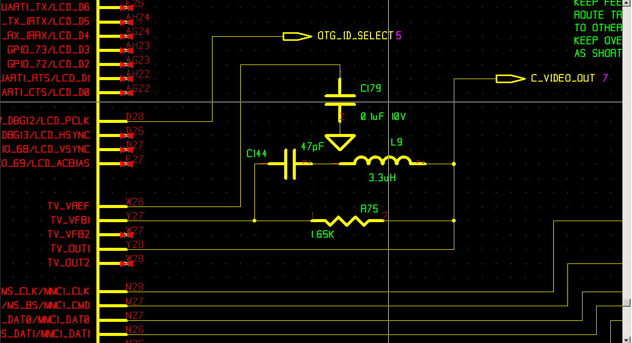
OMAP video feedback circuit

OMAP Video Feedback Circuit

Unfortunately, with the latest version of the OMAP silicon on the most recent boards, the video output, even with proper 75 ohm termination, was exhibiting nasty parasitics as shown below:
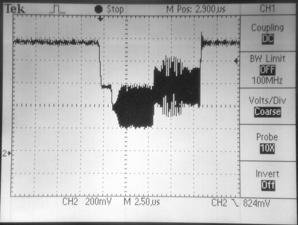
Angstrom video

Horizontal Interval

After creating a test schematic in Linear Tech’s LT Spice IV then running some analysis on it, this gave some indication of where the trouble might be.  As shown in the plot below the pole in the resonant circuit was around 12.7MHz, whereas the parasitics were between 16MHz to 19.3MHz.  After manipulating the values of R75 and C144 shown in the schematic above the pole in the response of the network moved out to about 20MHz.  After doing the plots and determining the component values it was time to modify the board.
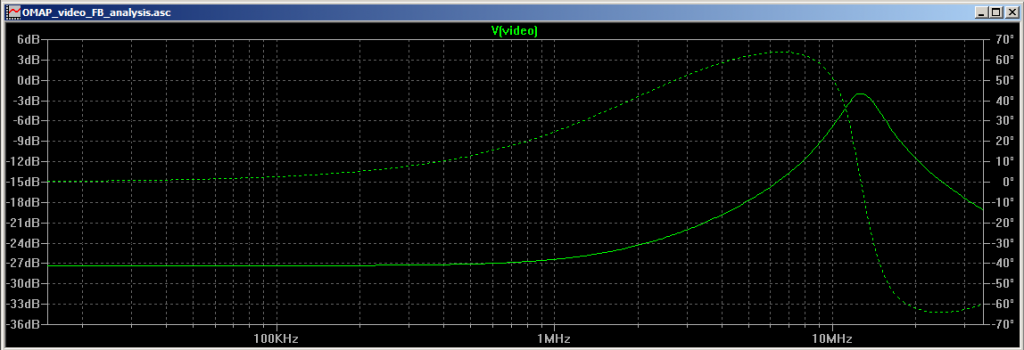
Spice Plot, Response of Feedback Network (original values)
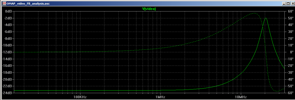
Spice Plot of Feedback Network, new values.

After modifying the board with new values for R75 (1.00K)  and C144 (18pF) we measured the video again.  Note that the baseline amount of feedback increased by about 4dB and the filter’s peak response narrowed somewhat.  Nonetheless now we can see that the video output is stable once again:
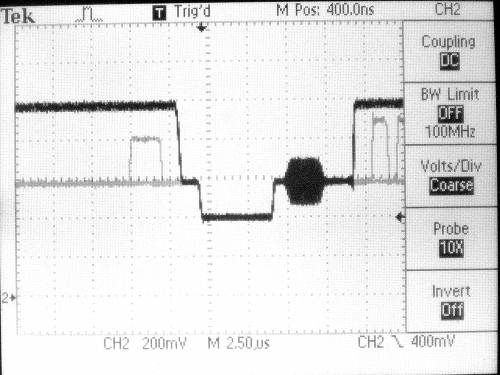
Horizontal Interval (NTSC) After Feedback Network Changes

The TI Technical Reference Manual for the OMAP processor mentions that the output amplitude of the peak to peak video signal is low, but they claim this is ok.  I beg to differ.   Indeed it is about 600mV to 700mV peak to peak, whereas NTSC video, sync tip to peak white, is 1.0Vpp.  Some TV’s can probably work with this for sure, but my Panasonic plasma display would not lock up to it.  I could see stuff parading across the screen but it always complained that there was no signal on the analog input.  So beware.  NTSC composite output is probably of little value anyway these days, except if you have a system like the Orion that has no other video display method.  But for this product video output is not a primary use case, so the video quality (or lack thereof) isn’t a show stopping concern.
Orion named one of the coolest demos at Google I/O 2011

LevelStar LLC’s Orion Braille enabled portable computing device was named one of the 16 coolest demos at Google I/O 2011. Read the whole article here. The Orion entry is here. The Orion contains 2 PCB’s and 3 flex circuits, all designed with CADSTAR. The main board is 8 layers, employing fine line design, blind and buried micro vias and lots of high speed design constraints. “I’ve used a number of CAD programs over the last 25 years, and can not imagine attempting to create a design like this without something like  Zuken’s CADSTAR.” said Jeff Sutherland, hardware architect for the Orion. “Zuken’s Board Modeler Lite proved to be crucial to the successful packaging of the product. There was a lot of back and forth with STEP models between us and the industrial design folks. Everything fit the first time around.” For more information about the Orion product, please contact LevelStar LLC.  Note that CADSTAR version 13, first released in November of 2011, now includes additional options for mechanical information interchange using IDF format files.

TI OMAP3530 Component Added To Library

Since Google was of no help to me in my latest project, I had to create a CADSTAR library component for the Texas Instruments OMAP3530 CPU chip.  The package is the CBB type, the 0.4mm BGA version used on the Beagleboard.  I’ve checked this over a couple of times but there could still be problems- never know about these until an actual board gets made.  I made the pin function descriptions on the symbols similar to those on the Beagleboard C4A revision schematics.  Note however there appear to be a couple of minor mistakes on the Beagleboard schematic when referencing the latest TI datasheet for the 3530 which was released late in 2009.

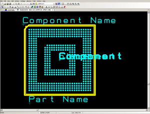
TI CBB footprint in CS library editor.

TI CBB (0.4mm 515) BGA Footprint

Reading through the TI appnotes for the CBB footprint you’ll find some interesting comments regarding its creation.  For one, they claim that below 0.5mm the rules change regarding metal defined pads verses solder mask defined (SMD) pads.  For 0.5mm and up it seems that metal defined pads typically give better yields, but TI claims that in their experiments with the 0.4mm package that SMD pads actually gave better yields.  Note also that only the outermost row of ball pads can be broken out on the surface.  All the inner rows must be broken out on the second or third layers using 4 to 6 mil via-in-pad blind vias.  TI also recommended filling the vias.  This could give your PCB vendor nightmares.  Works on the Beagleboard evidently, and in only 6 layers as well.  I’d also recommend using via-in-pad for the 6 outermost corner balls on each of the 4 outside corners as a way of reducing any chances of PCB pad cratering on those pins.  In another rule changing event, this footprint was created with the system units set to μm (yes, that’s MICRONS folks, it’s getting really crazy out there) which became available in CADSTAR release 12.

To help improve yields pay particular attention to making connections to the pads to avoid drawing heat away resulting in uneven soldering.  Do not use any trace wider than 0.2mm to attach any pad.  Be sure to see both parts I and II of the OMAP PCB assembly documentation at ti.com.

A zip file with the schematic symbols, the CBB footprint, and a library entry that lashes up all 515 of the balls can be downloaded here.  USE AT YOUR OWN RISK.  I have not proven this yet on a board.  If you don’t feel like living on the cutting edge then come visit us again in September to see how we got on with it.  Otherwise, dive in and get on with your OMAP design!

-Jeff