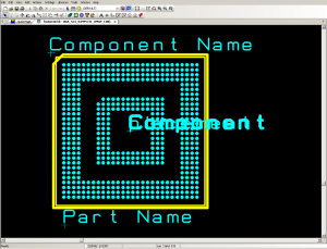
Since Google was of no help to me in my latest project, I had to create a CADSTAR library component for the Texas Instruments OMAP3530 CPU chip. The package is the CBB type, the 0.4mm BGA version used on the Beagleboard. I’ve checked this over a couple of times but there could still be problems- never know about these until an actual board gets made. I made the pin function descriptions on the symbols similar to those on the Beagleboard C4A revision schematics. Note however there appear to be a couple of minor mistakes on the Beagleboard schematic when referencing the latest TI datasheet for the 3530 which was released late in 2009.
Reading through the TI appnotes for the CBB footprint you’ll find some interesting comments regarding its creation. For one, they claim that below 0.5mm the rules change regarding metal defined pads verses solder mask defined (SMD) pads. For 0.5mm and up it seems that metal defined pads typically give better yields, but TI claims that in their experiments with the 0.4mm package that SMD pads actually gave better yields. Note also that only the outermost row of ball pads can be broken out on the surface. All the inner rows must be broken out on the second or third layers using 4 to 6 mil via-in-pad blind vias. TI also recommended filling the vias. This could give your PCB vendor nightmares. Works on the Beagleboard evidently, and in only 6 layers as well. I’d also recommend using via-in-pad for the 6 outermost corner balls on each of the 4 outside corners as a way of reducing any chances of PCB pad cratering on those pins. In another rule changing event, this footprint was created with the system units set to μm (yes, that’s MICRONS folks, it’s getting really crazy out there) which became available in CADSTAR release 12.
To help improve yields pay particular attention to making connections to the pads to avoid drawing heat away resulting in uneven soldering. Do not use any trace wider than 0.2mm to attach any pad. Be sure to see both parts I and II of the OMAP PCB assembly documentation at ti.com.
A zip file with the schematic symbols, the CBB footprint, and a library entry that lashes up all 515 of the balls can be downloaded here. USE AT YOUR OWN RISK. I have not proven this yet on a board. If you don’t feel like living on the cutting edge then come visit us again in September to see how we got on with it. Otherwise, dive in and get on with your OMAP design!
-Jeff

comment_form